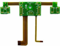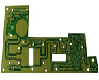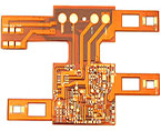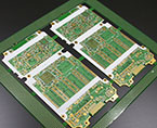


Rigid PCB Capability

|
Rigid PCB Capability |
||
|
No |
Item |
Technical data |
|
1 |
Number of Layers |
1-40Layers |
|
2 |
Max.Board Size |
508*610mm |
|
3 |
Board thickness |
0.2-5.0mm |
|
4 |
Min Line Width/Space |
4mil/4mil(0.1/0.1mm) |
|
5 |
Min.S/M Pitch |
0.1mm(4mil) |
|
6 |
Finish Drill Hole (Mechanical) |
0.2mm--6.30mm |
|
7 |
PTH Wall Thickness |
>0.020mm(0.8mil) |
|
8 |
Hole Dia.Tolerance(PTH) |
±0.075mm(3mil) |
|
9 |
Hole Dia.Tolerance(NPTH) |
±0.05mm (2mil) |
|
10 |
Hole Position Deviation |
±0.05mm (2mil) |
|
11 |
Outline Tolerance |
±0.10mm (4mil) |
|
12 |
Twist&Bow |
≤0.7% |
|
13 |
Insulation Resistance |
>1012Ω Normal |
|
14 |
Through hole resistance |
<300Ω Normal |
|
15 |
Electric strength |
>1.3 kv/mm |
|
16 |
Current breakdown |
10A |
|
17 |
Peel strength |
1.4N/mm |
|
18 |
S/M abrasion |
>6H |
|
19 |
Thermal stress |
288℃ 20 Sec |
|
20 |
Test Voltage |
50-300V |
|
21 |
Min. blind/buried via |
0.2mm/0.2mm(Mechanical) 0.1mm/0.2mm(Laser) |
|
22 |
Available Laminates Material |
CEM1, CEM3, FR-4, High-Tg FR4, Aluminum Base, Rogers, Taconic, Arlon etc. |
|
23 |
Finished board thickness tolerance |
T>=0.8mm, Tolerance: +/-8%, T<0.8mm : +/-10% |
|
24 |
Out Layer Copper Thickness |
1oz--6oz |
|
25 |
Inner Layer Copper Thickness |
1/2oz--4oz |
|
26 |
Aspect Ratio |
15:1 |
|
27 |
SMT Mini. Solder Mask Width |
0.08mm |
|
28 |
Mini. Solder Mask Clearance |
0.05mm |
|
29 |
Plug Hole Diameter |
0.2mm--0.60mm |
|
30 |
Impedance Control Tolerance |
+/-10% |
|
31 |
Surface Finish |
HASL,HAL(Lead free),Immersion Gold/Tin/Silver,Gold Plated, OSP, Gold Finger, Peelable mask |
|
32 |
Insulation Layer Thickness |
0.075mm--5.00mm |
|
33 |
Special technology |
Thick hard gold plating, Via in Pad, Counterbore&Countersunk etc. |